

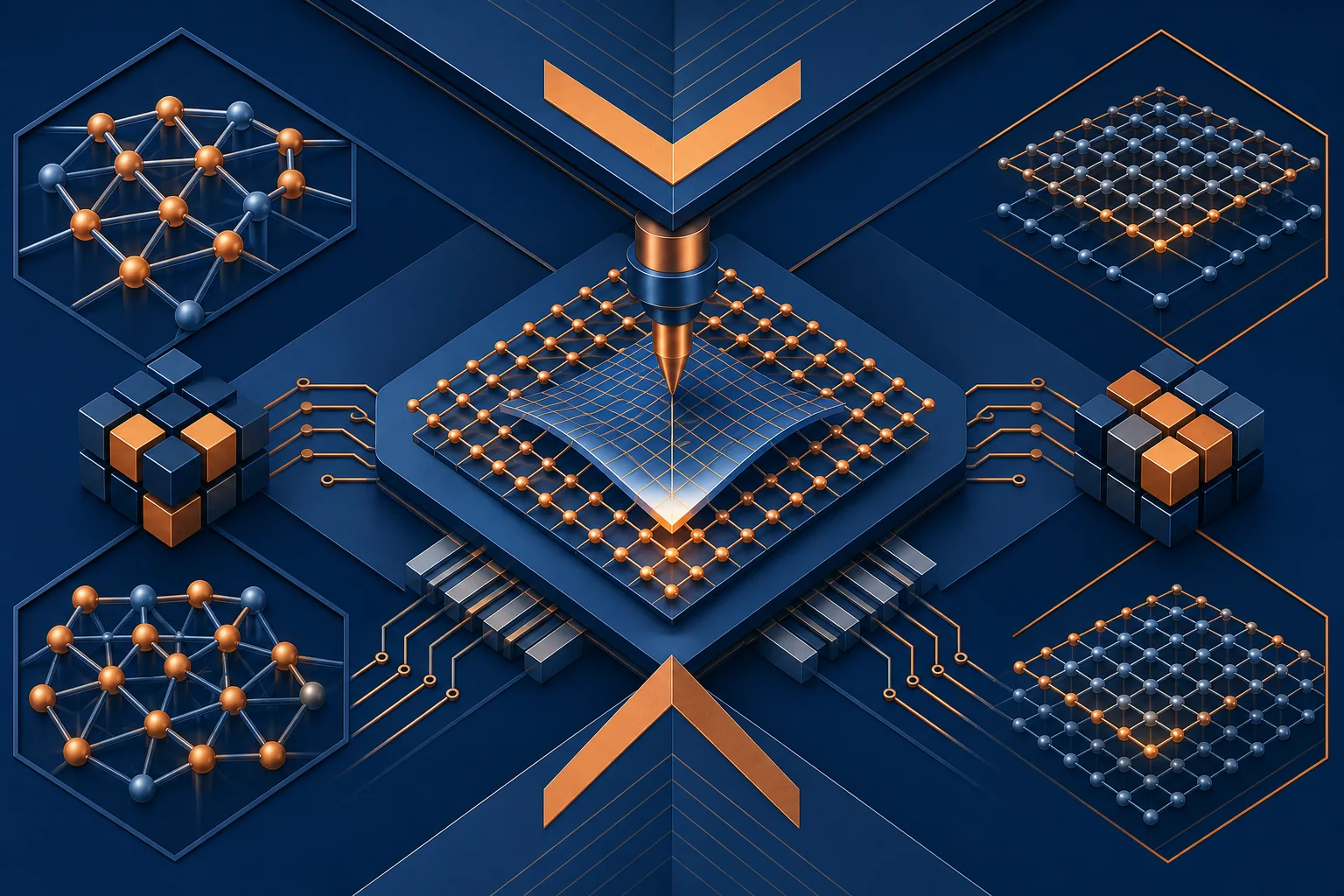
A research team led by Georgia Tech is developing a novel computing architecture that utilizes nanoscale mechanical strain to manipulate semiconductor logic states. This approach seeks to move beyond the traditional reliance on electrical charge movement, which has defined transistor performance for decades.
Asif Khan, an associate professor at the Georgia Tech School of Electrical and Computer Engineering, is spearheading the project. The research focuses on integrating multiple information-carrying modalities, including magnetism and mechanical strain, to represent binary data.
The initiative is supported by a $10.6 million grant from the Defense Advanced Research Projects Agency, specifically through its Fast and Curious program. This program mandates the development of logic circuits that achieve at least 100 times the energy efficiency of current state-of-the-art technologies.
The core technology, termed Mechanically Amplified Ferroic-Actuated (MEFA) Logic, employs ferroic materials that undergo physical deformation when subjected to voltage. This expansion or contraction is amplified and channeled into a semiconductor, effectively modulating current flow to toggle between logic states.
By utilizing the piezoelectric properties of these ferroic materials, the team can convert electrical input into precise mechanical displacement. This displacement exerts pressure on the semiconductor channel, altering the bandgap or carrier mobility to switch the device between high-conductance and low-conductance states.
Collaborators on this project include researchers from Rice University and the University of Southern California, who are providing expertise in materials science and device characterization. These academic partners are working alongside technical support from Northrop Grumman’s Space Park Foundry to ensure the fabrication processes align with industrial standards.
The Space Park Foundry contribution is particularly vital for the project, as the facility offers specialized capabilities in prototyping and testing advanced semiconductor materials. Their involvement helps bridge the gap between small-scale laboratory experiments and the rigorous requirements of high-volume manufacturing environments.
The team is prioritizing manufacturability and integration within the existing semiconductor ecosystem from the project’s inception. By ensuring compatibility with established fabrication processes, the researchers aim to avoid the adoption hurdles that often plague experimental computing technologies.
The project addresses the physical limitations inherent in complementary metal-oxide-semiconductor (CMOS) technology, which serves as the foundation for modern electronics. While CMOS has scaled effectively for years, its energy consumption remains a primary constraint for emerging high-performance computing applications.
Mechanical strain offers a pathway to tune the behavior of advanced materials, potentially reducing the energy required for switching operations. The research team intends to demonstrate that these mechanical forces can provide the necessary speed and functionality for real-world computational tasks.
The significance of this research lies in its potential to reconcile the demand for high-speed processing with the necessity for extreme energy efficiency. By shifting the mechanism of logic switching, the team hopes to create a viable alternative for future hardware architectures that must operate under strict power budgets.
The integration of ferroic-actuated logic represents a departure from purely electronic switching, introducing a hybrid physical-electronic paradigm. This methodology could prove critical for applications where thermal dissipation and power consumption are the primary bottlenecks for scaling.
Engineers must now prove that these devices can achieve sub-femtojoule switching energies while maintaining clock speeds competitive with current silicon-based transistors. The team is focused on demonstrating that the mechanical amplification factor remains stable across millions of cycles, a critical metric for long-term reliability in commercial logic circuits.
Future milestones for the project involve scaling from individual device demonstrations to the construction of complex, functional circuits. The team will continue to refine the amplification mechanisms to ensure the reliability and consistency required for commercial-grade semiconductor applications.
Observers will be monitoring the transition from laboratory prototypes to integrated circuit testbeds as the research progresses through the DARPA program timeline. The ability to integrate these ferroic materials into standard CMOS back-end-of-line processes will be the primary technical hurdle for the next phase of development.